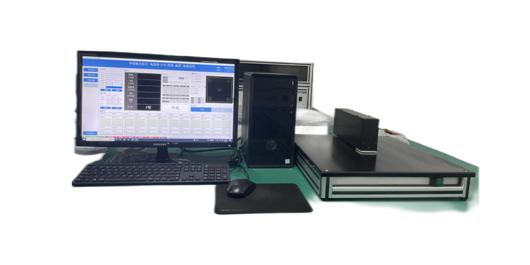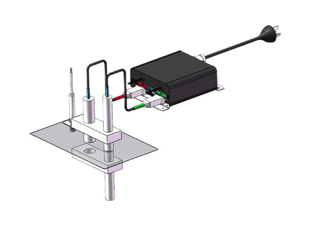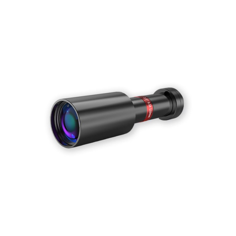

Three-In-One (Resistivity/PN/Temperature) Testing Module
Integration of resistivity, PN, and temperature
Option to integrate thickness probes
Mainly used in the photovoltaic field
CHARACTERISTICS
| Parameters | Sheet Resistance (Thickness approximately 100μm) | ||
| Probe Range | 6-2000Ω/(0.1-30Ω*cm) | ||
| Probe Performance | Dynamic Reproducibility | Static Reproducibility | Display Error |
| 006-080Ω/□(0.1-0.8Ω·cm)<0.15% | <0.02% | ≤±3% | |
| 080-160Q/□(0.8-1.6Ω·cm)<0.3% | <0.039% | ≤±3% | |
| 160-320Ω/□(1.6-3.2Ω·cm)<0.4% | <0.05% | ≤±3% | |
| 320-2000Ω/□(3.2-20Ω·cm)<0.5% | <0.1% | ≤±3% | |
| Dimensions | Upper Probe: φ20*145mm Lower Probe: φ20*100mm Control Box: 173*130*55mm | ||
| Signal Acquisition | Sampling Rate: ≤1ms, Data Acquisition >300 points Data Interface: RS232 RS485 CAN TCP/IP
Transmission Protocol: Modbus Rtu/Modbus Tcp, user-defined SOCKET protocol, etc. Automatic Temperature Compensation System Raw signals can be accessed openly |
||
DESCRIPTION
- This product integrates sheet resistance (resistivity), PN type, and temperature three probes for measurement. It can be widely used in photovoltaic and semiconductormeasurement fields such as silicon wafer sorting machines and production process analysis.
- PNTesting Principle (SPV Method) :Monochromatic light with energy greater than the semiconductor material bandgap width is irradiated onto the surface, generating electron-hole pairs inside the semiconductor material. Driven by concentration gradients, electrons and holes near the surface space charge region of the semiconductor material are separated by self-built electric fields, creating photo-generated voltage, known as surface photovoltage.

