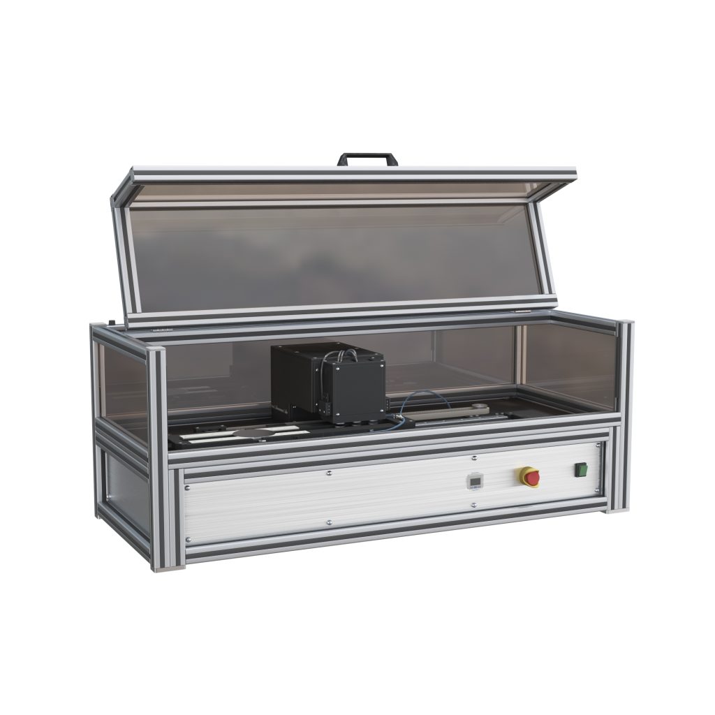

Resistance (Resistivity) Tester (Wafer and Ingot)
non-contact and non-destructive, with advantages of fast testing speed, good repeatability, high testing sensitivity, allowing direct testing of product wafers
CHARACTERISTICS
| Parameters | Probe | Resistance Range | Resistivity Range | Testing Method |
| Range | Low-resistance probe | 0.005-1Ω/□ | 0.25-500mΩ*cm | Eddy current method, non- contact |
| Mid-resistance probe | 0.05-10Ω/□ | 2.5-500mΩ*cm | ||
| High-resistance probe | 10-3000Ω/□ | 0.5-150mΩ*cm | ||
| Ingot probe | 0.01-2Q*cm | |||
| Repeatability | <0.2%(≤50% range) | <0.5%(>50% range) | ||
| Accuracy | <2%(≤50% range) | <3%(>50% range) | ||
| Probe Information | Type of Probe: Dual-probe (upper and lower probes with a 2-3mm gap), Probe Diameter: Outer diameter 20mm, Inner diameter 14mm (effective testing part), Probe Gap: 30mm | |||
| Coordinate Settings | Arbitrary Coordinate Settings | |||
| Store data | Internal Database Storage (Exportable Table Files),
PDF Test Report containing test information (time, operator), wafer information (number, size, thickness), data information (number of test points, max/min/average values, relative standard deviation, etc.), contour maps, surface maps, etc. CSV Table Data Storable to Remote Server Modifiable report information as per customer requirements |
|||
| WAFER
Information |
Size: 2”-8” (inches) | Thickness:100-1500mm | ||
| System Requirements | Power Supply: AC220V,50/60Hz Relative Humidity:20%-80%RH | Power: 600W Environment: Temperature 24℃±10℃ Size: 975*465*425(mm) Lifespan: >10 years | ||
| Material | Resistivity | Sheet Resistance |
| Silicon wafer | Y | Y |
| Sic wafer /Ingot | Y | Y |
| GaO wafer /Ingot | Y | Y |
| GaN wafer 2DEGI | Y | Y |
| GaAs 2EDG | Y | |
| GZO/LTPS/ITO | Y | |
| flat panel) | Y | |
| TCO(Touch panel) | Y | |
| Graphene | Y | |
| Metal film |
DESCRIPTION
- The equipment primarily utilizes eddy current testing principles to test the sheet resistance (resistivity) of semiconductor materials, graphene, transparent conductive films, carbon nanotubes, metals, and other materials without physical contact. It enables single-point and area scanning tests, used for material research and process monitoring for quality control purposes.
- When a detection coil carrying an alternating current approaches the tested conductor, due to the coil’s alternating magnetic field, eddy currents are induced in the tested conductor, creating a magnetic field opposite to the original magnetic field, partially offsetting the original magnetic field, resulting in changes in the resistance and inductance of the detection coil.
- Resistivity = Sheet Resistance * Wafer Thickness Sheet Resistance and V have a relationship
Resistivity is used to represent the electrical resistance characteristics of a material, it is a physical quantity of the material’s electrical properties.

