Solutions
Photovoltaic Silicon Wafer Detection
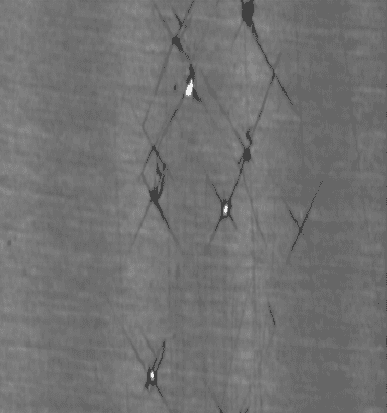
to detect the chips, cracks, or concentric circles.
Our customers want to know are there chips, cracks, inside cracks, or concentric circles on or in their silicon wafers, which will decrease the photoelectric conversion efficiency.
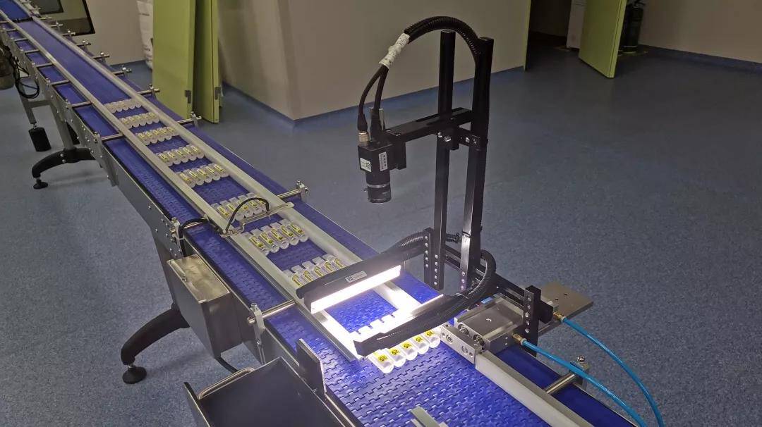
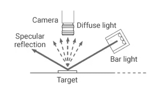
Our solution is : use the high resolution line scan cameras and lens, which can cover 30cm field of view, at the same time, use the high brightness linear light source to light the products.
The products passes through the conveyor belt at a constant speed and the image is captured and analyzed by the line scan camera.

The detection figure :

Share the Post:

